Since the beginning of the 21st century, the communication industry has been challenged by the ever-increasing demands for bandwidth and speed. Large-capacity and high-speed optical fiber communication have become an inevitable trend in the development of the information age. As the core components of optical fiber communication networks, the technological development of optical transceiver modules is also becoming more and more mature and gradually developing in the direction of high speed, intelligence and miniaturization.
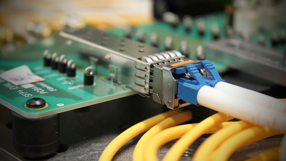
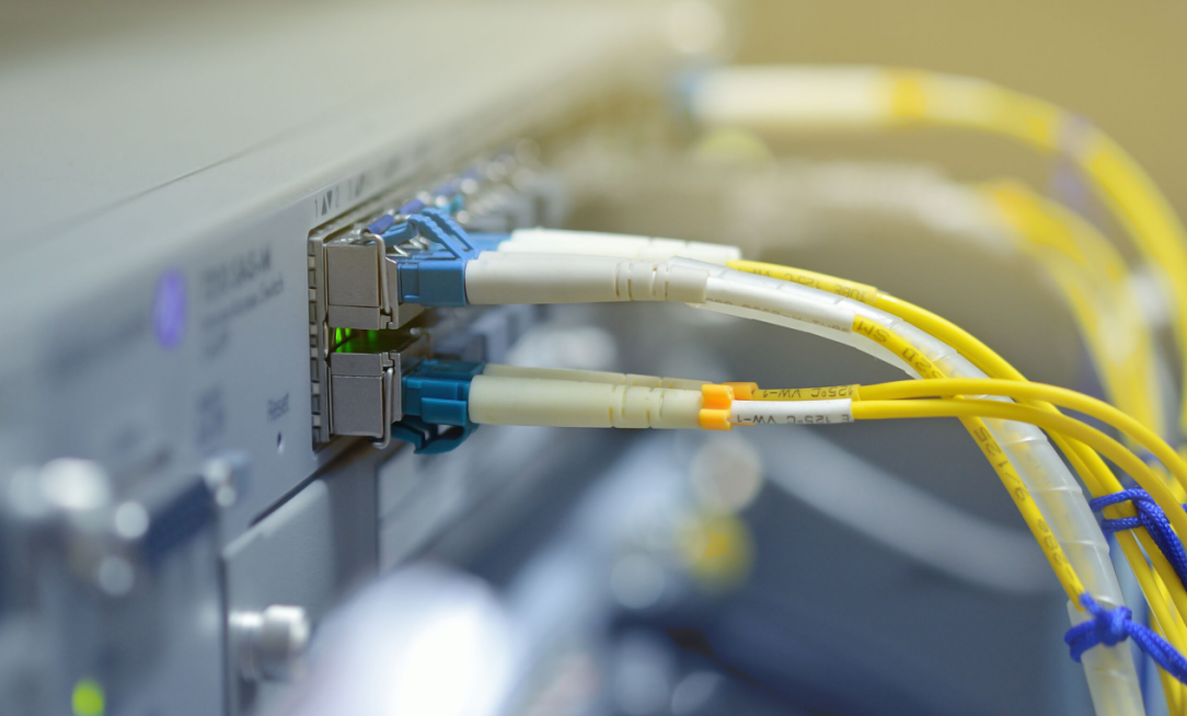
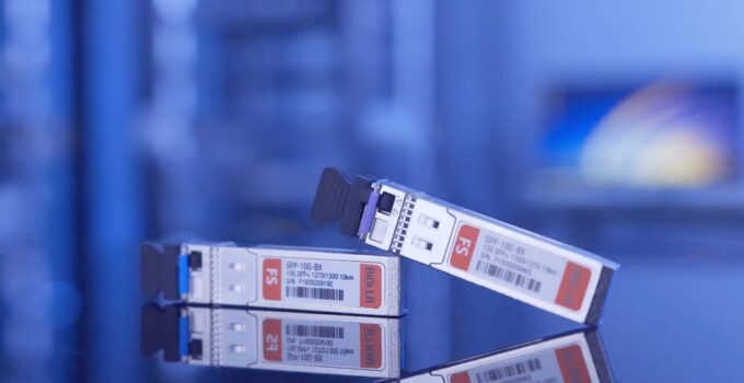
The optical transceiver module mainly completes the optical-electrical/electrical-optical conversion function of optical signals and integrates transmission, reception, various functional circuits, standardized optical fiber connectors, and electrical signal interfaces to form a high-speed integrated system module. At present, the optical transceiver module technology with a transmission rate of 2.5 Gb/s has matured, and the 10G SFP+ optical transceiver (click here) technology has begun to be widely used. The circuit design trend of the 10G SFP+ optical transceiver (FS.COM) is taken as an example below.
As the optical transceiver module develops towards high speed, its design difficulty also increases accordingly. To integrate light-emitting, light-receiving, and digital diagnostic circuits on a very small circuit board, the signal integrity issues brought about by high-speed signals must be fully considered. Therefore, the simulation analysis method must be used to assist the high-speed circuit design.
10G optical module high-speed circuit design method

Source: fs.com
The traditional PCB design method is usually to test the circuit board prototype through a series of instruments to verify the success of the design. Once a problem is found, it needs to be revised and debugged again. This method makes the product development and design cycle long, the time to market the product is uncontrollable, and the development cost caused by multiple revisions is also high. Traditional PCB design methods are no longer suitable for modern high-speed PCB design, and the introduction of high-speed circuit design methods based on signal integrity theory and software-assisted simulation tool analysis has become inevitable. The development process of high-speed PCB design mainly has the following steps.
(1) System design stage: consider systematically as a whole, and adopt a design scheme that avoids signal integrity risks;
(2) Classify the signals on the target PCB, identify potential risks, and determine the overall design principles;
(3) Schematic design: take certain measures in advance to avoid signal integrity problems;
(4) Analysis before wiring: use simulation tools to quantify various performance indicators of the signal and formulate detailed design rules;
(5) Simulation after wiring: Use simulation tools to verify the performance indicators of the signal, and modify and optimize. In the new design method, each stage includes the signal integrity design link, which can effectively solve all possible signal integrity problems before the finished product is produced, thereby greatly shortening the product development cycle, reducing the cost of multiple revisions, and ensuring Product design success rate.
Simulation and Analysis of Optical Transceiver Module Circuit
With the development of optical transceiver modules in the direction of high speed, in the PCB design of 10G optical modules , the problem of signal integrity is becoming more and more obvious. The two parts of differential signal and optical device lead design are extremely critical to the optical module. The following simulation analysis is carried out for the above two parts.
Simulation of Differential Signals

With the rapid development of high-speed circuits, the application of differential signals has become more and more extensive. The typical differential signal interfaces include LVDS/CML/LVPECL. Most of high-speed circuits currently use differential signal interconnection design.
In a differential signal interconnect design, two transmission lines are used to transmit the signal. A differential driver has two outputs that output signals simultaneously. Ideally, the edges of the two signals are aligned, but the inversion directions are opposite. The two signals are transmitted along their respective transmission lines. When they reach the receiver, the receiver performs differential detection on the two signals and extracts the difference from the two signals. information, this difference signal is called differential signal. Compared with ordinary single-ended signal traces, differential signals can well solve the problem of different potentials at the sending and receiving reference points, and have the stronger anti-interference ability under certain conditions.
In the 10G optical module PCB, a differential signal interconnection design is adopted. The differential signal is connected to the connector through a capacitor. The spacing of the pads in the two differential lines is an important parameter for optimization. The parameterized model is established in HFSS.
Simulation of Optical Device Leads

Source: etulinktechnology.com
The 10G SFP+ optical transceivers also have different requirements for transmission distance and wavelength in different application scenarios (learn more). Usually, the performance of optical devices (including laser and detector components) is a key factor determining the quality and reliability of the eye diagram of an optical transceiver module. As the lead connecting the optical module PCB and the optical device, it is also an important content that needs to be paid attention to in the signal integrity design of the optical module.
Compared with the PCB, there is a big difference, so to reduce this discontinuity, simulation must be carried out to find the influencing factors and the direction of optimization. Usually, the lead wire of the optical device is made of copper-clad gold material, and its thickness cannot be changed after leaving the factory, but its lead wire length and solder joint position can be adjusted within a certain range.
By changing the lead length of the optical device, the experimental conclusion is drawn that the lead length of the optical device has a great influence on the transmission quality of the signal, and the length of the optical device lead should be as short as possible, which is the parasitic inductance brought by the lead. caused by. In addition, as the lead wire is shorter, the signal is more sensitive to the lead wire length, and the reflection characteristic fluctuates greatly, which requires the lead wire of the optical device to be strictly controlled to be equal in length when it is connected. On the other hand, the position of the optical device lead pad is as close as possible to the inner side of the pad, because the part in contact with the pad increases the reflow path. In summary, the length of optical device leads and the position of solder joints have a significant impact on the overall performance of the optical module. The above simulation results provide important reference values in the actual design and welding process of the optical module.
Conclusion
With the continuous improvement of the circuit speed of optical transceiver modules, the problems of signal quality and delay caused by interconnection and devices have become increasingly prominent, and circuit design engineers have to face serious signal integrity problems. At present, the signal integrity of high-speed circuit design has become a new field, and the high-speed circuit design method based on signal integrity theory and software-assisted simulation tool analysis is undoubtedly a great challenge for circuit design engineers.


